

1. What Is a (551) Silicon Wafer? How Is It Different from a Conventional <100> Wafer?
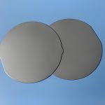
A (551)-oriented silicon wafer (a high-index orientation wafer), written in standard notation as the (551) plane / <551> direction, is a high-index off-axis silicon — not a mass-production generic orientation (the usual ones are 100/111/110). This kind of special-orientation wafer is generally not kept in stock and is mainly made to order.
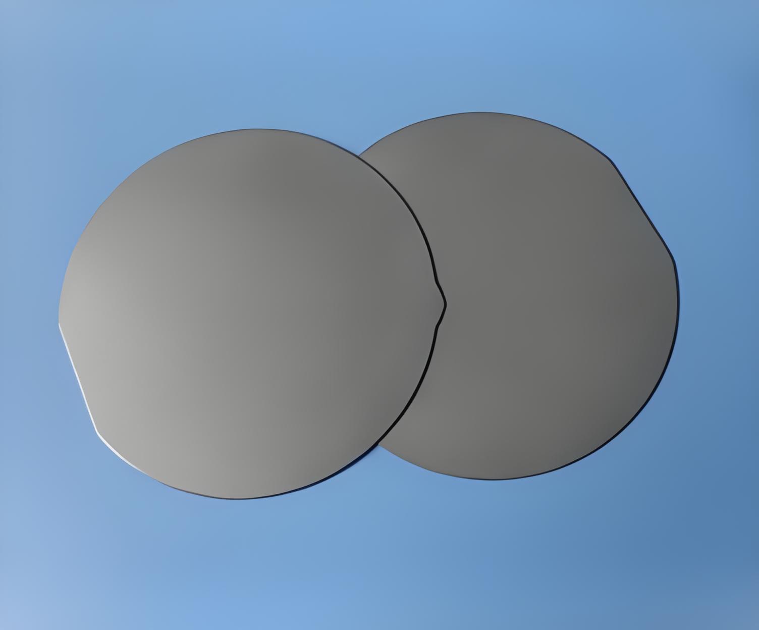
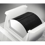
2. Specification Sheet — 4-Inch, 0.2mm-Thick (551) Silicon Wafer
CERTIFICATE OF ANALYSIS
| PRODUCT | Double-Side Polished Wafer | SUPPLIER | Huoying Technology |
|---|---|---|---|
| Lot No. | X00126052201 | QTY | 25 pcs |
| PARAMETER | REQUEST | SAMPLE DATA | |
| Growth Method | FZ | FZ | |
| Type | – | – | |
| Dopant | – | – | |
| Resistivity (ohm-cm) | >3000 | 3200–4300 | |
| Crystal Orientation | <551> | <551> | |
| Off Orientation (°) | ±0.2 | ±0.2 | |
| Diameter (mm) | 100 ± 0.2 | 100.0–100.1 | |
| Primary Flat Length (mm) | 32.5 ± 2.5 | 32.5 ± 2.5 | |
| Secondary Flat Length (mm) | – | – | |
| Thickness (µm) | 200 ± 5 | 199–203 | |
| TTV (µm) | <5 | 1.6–2.7 | |
| Bow (µm) | <10 | 1.3–2.4 | |
| Warp (µm) | <15 | 8.8–11.2 | |
| Particle (# @ >0.3 µm) | – | – | |
| Frontside Finish | Polished | Polished | |
| Backside Finish | Polished | Polished |
3.<551> vs. Conventional <100> Orientation Comparison
| Orientation | Positioning | Typical Applications |
|---|---|---|
| (100) | Mass-production mainstream | CMOS, general MEMS, pressure sensors |
| (111) | Power devices / optoelectronics | IGBT, silicon photodetectors |
| (110) | Special-mobility devices | Some MOS, micro-mirrors |
| (511) | High-index (commercially mature) | XRD zero-background substrates |
| (551) | High-index custom R&D | Fin devices, special 3D etching, surface research |
4. Mechanical & Physical Properties of (551) Silicon Wafers
For (551) silicon wafers, the fixed charge of the SiO₂/Si interface and the interface state density lie between those of (100) and (111). Carrier mobility is strongly anisotropic, with markedly different transport along different orientations. Ion implantation and impurity diffusion rates depend on the surface step structure and differ from the diffusion profiles of low-index wafers. The elastic modulus and Poisson’s ratio of silicon vary significantly with orientation; (551) is commonly used in stress-engineered devices, micro-resonators, and piezoelectric / piezoresistive MEMS simulation and sample preparation.
5. Applications of (551) Silicon Wafers
FinFET, gate-all-around (GAA) and nanosheet transistor experiments — (551) sidewalls are used to optimize channel mobility; a large number of semiconductor process patents use this orientation substrate.
Anisotropic wet etching to fabricate unconventional inclined micro-grooves, micro-mirrors, blazed gratings and 3D microstructures, for prototype devices that require precise control of sidewall inclination.
Periodic step surfaces used as model substrates for studying metal epitaxy, 2D material growth, surface reconstruction and adsorption kinetics.
For XRD zero-background substrates, (510) and (511) are the preferred choices; the diffraction peak position of (551) is not suitable for removing substrate interference in conventional powder XRD — do not pick the wrong one.
6. Which Special-Orientation Silicon Wafers Does Guizhou Huoying Technology Offer?
We can custom-manufacture the following special-orientation silicon wafers: (551), (553), (533), (311), (750), (733), (754), (331), (320), (730), (211), (310), (664), (755), (410) and more. If you have any special requirement, please contact the website customer service for consultation.