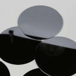


What Is an InAs Substrate?
Indium arsenide (InAs) is a III-V compound semiconductor material with a bandgap of approximately 0.354 eV at room temperature — one of the narrowest bandgaps among mainstream compound semiconductors. InAs offers exceptionally high electron mobility (intrinsic mobility above 20,000 cm²/V·s) and very low electron effective mass, giving it a decisive advantage in high-speed electronic devices and infrared detection.
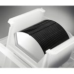
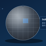
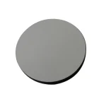
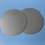
InAs single crystals are typically grown by the vertical Bridgman (VB) or float-zone method, then sliced, ground, and polished into wafers. The mainstream commercial formats today are 50 mm (2-inch) and 76 mm (3-inch) diameter wafers with a (100) orientation and a thickness of approximately 500 μm, available as single-side polished (SSP) or double-side polished (DSP), with custom specifications available on request.
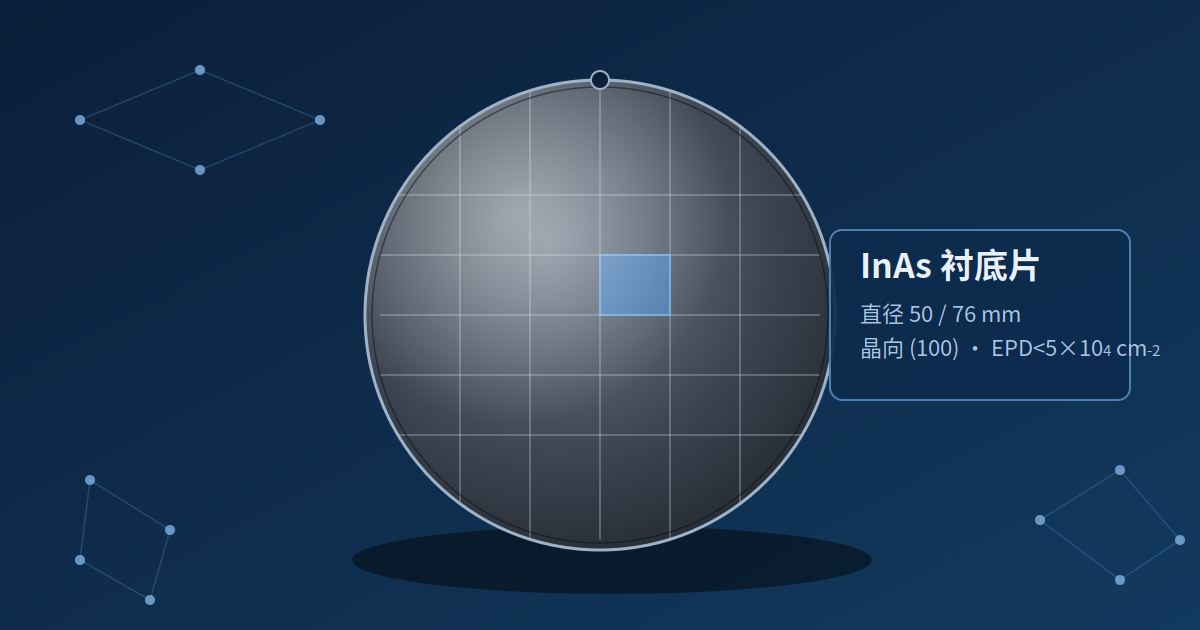
Key Specifications of InAs Wafers
The table below summarizes a typical InAs wafer specification, covering undoped material and three common doping options for easy side-by-side comparison:
| Dopant | Diameter (mm) | Conductivity Type | Carrier Concentration (cm⁻³) | Mobility (cm²/V·s) | Dislocation Density, EPD (cm⁻²) |
| Undoped InAs | 50/76 | N-type | 5×10¹⁶ | ≥2×10⁴ | <5×10⁴ |
| Sn-InAs | 50/76 | N-type | (5–20)×10¹⁷ | >2,000 | <5×10⁴ |
| S-InAs | 50/76 | N-type | (1–10)×10¹⁷ | >2,000 | <5×10⁴ |
| Zn-InAs | 50/76 | P-type | (1–20)×10¹⁷ | 100–300 | <5×10⁴ |
Standard specifications: single-side or double-side polished, (100) orientation, thickness 500 ± 25 μm; other special requirements can be satisfied on request.
Undoped InAs: The Baseline Choice for Epitaxy
Undoped InAs has a carrier concentration of about 5×10¹⁶ cm⁻³ and a mobility of no less than 2×10⁴ cm²/V·s. It should be noted that, due to InAs’s inherently high background carrier concentration, it does not behave like semi-insulating GaAs. Undoped wafers are primarily used as baseline substrates for epitaxial growth — ideal for epitaxial processes that are sensitive to dopant species and for fundamental research.
Sn-InAs and S-InAs: Two N-Type Doping Routes
- Sn-InAs: carrier concentration of (5–20)×10¹⁷ cm⁻³. Tin is the most commonly used donor dopant in InAs, offering stable, uniformly distributed doping levels. It is well suited as a substrate for epitaxial buffer layers and for ohmic-contact-related device structures.
- S-InAs: carrier concentration of (1–10)×10¹⁷ cm⁻³. Sulfur doping also yields N-type conductivity with a wider concentration window, providing more flexibility for mid- and low-concentration N-type applications.
Both offer mobility greater than 2,000 cm²/V·s, with dislocation density controlled below 5×10⁴ cm⁻² — fully meeting the crystal-quality requirements of most epitaxial devices.
Zn-InAs: The P-Type Doping Solution
Zinc is a typical acceptor impurity in InAs. Zn-InAs wafers have a carrier concentration of (1–20)×10¹⁷ cm⁻³, P-type conductivity, and a mobility of 100–300 cm²/V·s. P-type InAs substrates are indispensable for heterojunction bipolar transistors (HBTs), P-type contact layers, and related optoelectronic device structures.
Dislocation Density (EPD): The Hidden Gatekeeper of Epitaxial Quality
All four product types in the table have an EPD below 5×10⁴ cm⁻². Dislocation density directly determines the crystal quality of quantum wells and superlattices grown on top, which in turn affects the dark current and responsivity of infrared detectors. When purchasing, always request a recent EPD etch-pit test report from the supplier rather than relying solely on the datasheet.
Main Applications of InAs Substrates
Infrared Detectors and Focal Plane Arrays
The InAs bandgap corresponds to the 3–3.5 μm mid-wave infrared band. Detectors based on InAs/InAsSb superlattices are an important alternative to HgCdTe technology, widely used in gas sensing (absorption lines of CH₄, CO₂, and other molecules), industrial temperature measurement, and security monitoring.
High-Frequency, High-Speed Electronic Devices
With its high electron mobility and narrow bandgap, InAs and InGaAs/InAs heterostructures are preferred materials for high-electron-mobility transistors (HEMTs), used extensively in millimeter-wave communication, low-noise amplifiers, and other RF front ends.
Quantum Devices and Spintronics
InAs enables the growth of InAs/GaSb type-II superlattices, InAs quantum dots, and related structures, making it a key platform material for mid-infrared lasers, quantum cascade lasers, and spintronics research.
Buffer Layers and Substrate Engineering
InAs is also widely used as a buffer layer or virtual substrate for the epitaxy of ternary and quaternary alloys such as InAsSb and InGaAsSb, helping to relieve lattice mismatch and improve device-layer quality.
Five Key Considerations When Buying InAs Substrates
- Match conductivity type and doping to your epitaxial design: choose undoped or Sn/S-doped substrates for N-type structures, and Zn-InAs for designs with P-type contact layers; always verify the doping window against your epitaxy design documents.
- Wafer diameter and production-line compatibility: 50 mm and 76 mm are the standard sizes. 76 mm wafers significantly increase die output per epitaxial run and lower unit cost — but confirm your equipment fixture compatibility first.
- Polishing and surface quality: SSP is suitable for general epitaxy; DSP is preferred for devices requiring optical access through the backside or transparent-window applications. Pay attention to surface roughness, scratches, and haze defects.
- Custom capability for orientation and thickness: the standard orientation is (100) with a 500 ± 25 μm thickness. For (111)/(110) orientations or other thicknesses, confirm the supplier’s lead time and price adjustment.
- Lot-to-lot consistency and traceability: InAs contains indium and arsenic, the price is relatively high, and batch variation directly affects epitaxial yield. Request carrier concentration, mobility, and EPD test data for each lot, and perform incoming inspection when necessary.
Frequently Asked Questions (FAQ)
Q1: How does an InAs substrate differ from GaAs and InP substrates? A: InAs has the narrowest bandgap (about 0.354 eV) and the highest electron mobility, making it ideal for mid-wave infrared and high-frequency devices. GaAs (1.42 eV) dominates general RF and optoelectronic applications, while InP (1.34 eV) is the material of choice for optical-communication lasers and photodetectors. The three also have different lattice constants and therefore different epitaxial-matching partners.
Q2: Is undoped InAs a semi-insulating substrate? A: No. InAs has a high background donor concentration, so undoped wafers are still N-type (about 5×10¹⁶ cm⁻³). Unlike semi-insulating GaAs, InAs cannot be used as a high-resistivity substrate — don’t confuse the two when specifying.
Q3: How do I choose between Sn doping and S doping? A: Both are N-type. Sn doping offers higher and more stable concentrations ((5–20)×10¹⁷ cm⁻³), ideal for low-resistance buffer layers. S doping offers a wider range ((1–10)×10¹⁷ cm⁻³), better suited to applications needing moderate concentration with good mobility. Final selection should be validated by simulation and experiments on your specific epitaxial structure.
Q4: How should InAs wafers be stored and shipped? A: Wafers are typically vacuum-sealed or packaged under inert gas. Store them in a dry nitrogen cabinet with stable temperature, avoiding rapid thermal cycling. The InAs surface is relatively oxidation-sensitive, so use wafers soon after opening; always handle with cleanroom gloves and a vacuum wand.
Q5: Is an EPD below 5×10⁴ cm⁻² good enough? A: Yes — this is the mainstream industry specification for most InAs-based infrared detectors and HBTs. For structures that are extremely dislocation-sensitive, such as quantum-dot lasers, stricter custom specifications can be negotiated with the supplier.
Q6: Can other diameters, orientations, or polish finishes be customized? A: Yes. Beyond the standard 50/76 mm sizes, special diameters, (111) and other orientations, double-side polishing, and non-standard thicknesses are all commonly available as custom orders — just confirm the lead time before ordering.
Q7: What is the general price level of InAs wafers? A: InAs wafers are considerably more expensive than GaAs and InP substrates, and prices fluctuate with indium prices and specifications. Undoped wafers are the most economical, while doped and double-side-polished wafers carry a premium. Please contact your supplier for a real-time quotation.
Summary and Selection Guide
With its narrow bandgap and high electron mobility, InAs holds an irreplaceable position in mid-wave infrared detection, high-frequency electronics, and quantum-structure epitaxy. A practical decision path for buyers:
- Infrared superlattice / quantum-well epitaxy: choose undoped InAs, focusing on EPD data and lot consistency;
- N-type low-resistance buffer layers and ohmic contacts: choose Sn-InAs for its higher, more stable concentration ceiling;
- Moderate-concentration N-type applications: choose S-InAs for a good balance of mobility and concentration flexibility;
- P-type contact layers or P-type structures: choose Zn-InAs — its lower mobility is normal and expected;
- Cost reduction in volume production: upgrade from 50 mm to 76 mm where possible to increase output per wafer.
If you need InAs substrates, InAsSb, or other III-V materials in custom specifications, feel free to contact us for the latest datasheet and quotation. We offer single-side/double-side polished wafers, multiple orientations, and custom doping concentrations tailored to your requirements.
FZ/MCZ Growth Siliocn Wafer SiC Epitaxy wafer & substrate 2-8inch SiC bulk wafer Single-Crystal Silicon Wafers: The Foundation of Modern Electronics 6-Inch Sapphire Wafer: Price, Providers, and Manufacturer Direct Trends 2025