

1. What Is a Float Zone (FZ) Silicon Wafer? How Is It Manufactured?
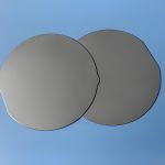
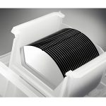
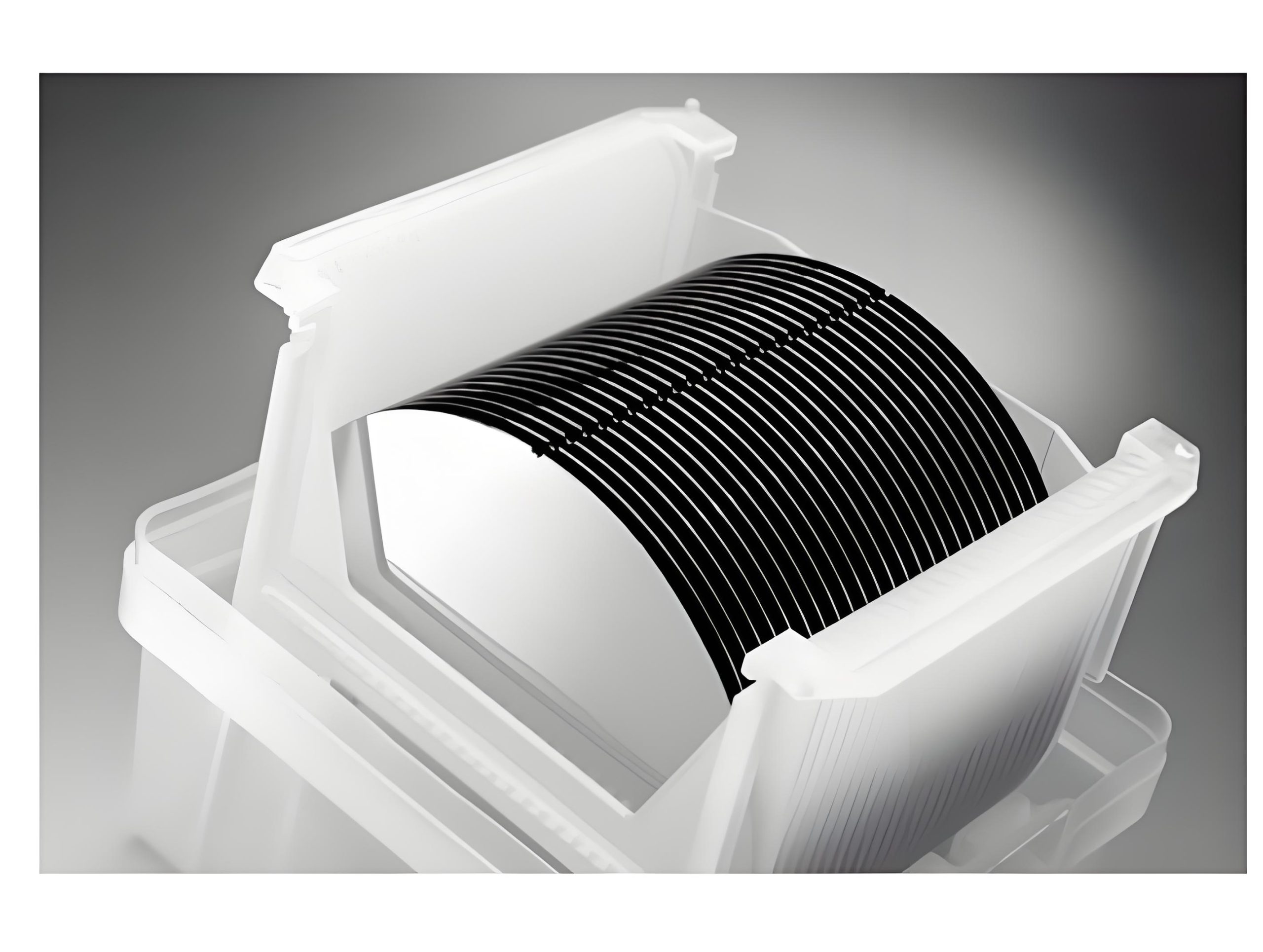
A float zone silicon wafer is a single-crystal silicon wafer produced by growing a float zone single-crystal silicon ingot using the float zone (FZ) method, and then processing the ingot into wafers. Because the silicon material is suspended during crystal growth and never comes into contact with a quartz crucible, it suffers far less contamination during growth. As a result, FZ wafers have lower carbon and oxygen content, fewer impurities and higher resistivity, making them well suited to power devices and certain high-voltage electronic devices.
During crystal growth, FZ silicon wafers are generally not doped with impurity elements such as boron or phosphorus the way Czochralski (CZ) wafers are. Therefore, most FZ wafers are intrinsic, undoped high-resistivity wafers with resistivity greater than 1000 Ω·cm. In some cases, however, the FZ ingot can be doped by neutron transmutation doping (NTD) or gas-phase doping to achieve better uniformity and lower resistivity.
In summary: a float zone wafer (FZ wafer) is a single-crystal silicon wafer prepared by the float zone (FZ) method. Its core characteristics are no crucible contact, extremely high purity, low oxygen and carbon content, and high resistivity.
2. FZ vs. CZ — Core Comparison Table
| Comparison Aspect | FZ Silicon Wafer | CZ Silicon Wafer |
|---|---|---|
| Core process | Float zone method: no crucible contact; high-frequency induction heating forms a floating molten zone; polycrystalline rod grows vertically | Czochralski method: poly-Si is melted in a quartz crucible; seed crystal is dipped into the melt and pulled vertically |
| Material purity | Impurities at ppb level (10⁻⁹); can be further purified by multiple zone passes; extremely high purity | Impurities at ppm level (10⁻⁶); high purity but limited by crucible contamination |
| Oxygen content | As low as 10¹⁴ atoms/cm³, 1–2 orders of magnitude lower than CZ; almost no oxygen-related defects | Typically 10¹⁶–10¹⁸ atoms/cm³; higher oxygen content, prone to oxygen-related defects |
| Resistivity range | Usually 1000–20000 Ω·cm; ultra-high resistivity achievable, suited to high-voltage applications | Generally <100 Ω·cm; mainly low-to-medium resistivity, suited to conventional semiconductor applications |
| Crystal quality | Very few dislocations, stacking faults and other defects; long minority carrier lifetime (>1000 μs); excellent crystallographic integrity | Fewer crystal defects; minority carrier lifetime typically tens to hundreds of μs; good crystallographic integrity |
| Main sizes | 4–6 inches (100–150 mm); large-diameter wafers are difficult to produce due to process limits | 6–12 inches (150–300 mm); large-diameter mass production possible, up to 18 inches |
| Key applications | High-voltage power devices (IGBT, thyristors, high-voltage MOSFETs), RF/microwave devices, semiconductor radiation detectors, infrared detectors, specialty radiation-tolerant PV cells | General integrated circuits, logic chips, memory chips, conventional power devices, consumer PV cells, LED chips — the vast majority of semiconductor applications |
| Cost & market share | Complex process, higher cost; approx. 15% of the global single-crystal silicon wafer market | Mature process, low cost, strong mass-production capability; approx. 85% of the global single-crystal silicon wafer market |
3. FZ Silicon Wafer Parameter Table
| Diameter | 2″ | 3″ | 4″ | 5″ | 6″ | 8″ |
|---|---|---|---|---|---|---|
| Growth Method | FZ | |||||
| Orientation | <100>, <111> | |||||
| Type / Dopant | Intrinsic, N-Type/Phos, P-Type/Boron | |||||
| Thickness (µm) | 279 | 380 | 525 | 625 | 675 | 725 |
| Thickness Tolerance | Standard ±25 µm | ±50 µm | ||||
| Resistivity (Ω·cm) | 1000–20000, Maximum Capabilities >20000, and 1–5 | |||||
| Surface Finish | P/E, P/P, E/E, G/G | |||||
| TTV (µm) | Standard <10 µm | |||||
| Bow / Warp (µm) | Standard <40 µm | <50 µm | ||||
| Particle | <10 @ 0.3 µm |
We offer premium FZ silicon wafers, low-stress silicon nitride wafers, a range of high- and low-resistivity silicon wafers, and single-crystal silicon wafers. If you have any requirement, please contact the customer service on this page via WeChat.