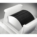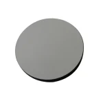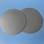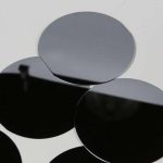


In RF devices, power semiconductors, MEMS, and various detector R&D applications, conventional CZ (Czochralski) silicon wafers often fall short. That is where float-zone (FZ) high-resistivity silicon wafers come in. A recent batch of 4-inch FZ single-side polished (SSP) wafers has been packed and shipped, and this article uses that batch as a real-world example to explain the key parameters, applications, and buying considerations of high-resistivity silicon wafers — all in one place.
What Are FZ High-Resistivity Silicon Wafers?
FZ wafers are made from monocrystalline silicon grown by the float-zone (FZ) method. Unlike the common Czochralski (CZ) process, the float-zone method uses no quartz crucible: the molten zone is suspended between the polysilicon rod and the monocrystalline seed, melting and recrystallizing segment by segment. Because the silicon never touches a quartz crucible, oxygen content is extremely low and purity is exceptionally high. With so few impurities, FZ wafers can achieve resistivity levels that CZ wafers simply cannot reach — this batch, for example, has a resistivity above 20,000 Ω·cm, a typical high-resistivity specification.
What Does High Resistivity Actually Mean?
Resistivity is the core measure of a wafer’s electrical conductivity. Standard CZ polished wafers typically range from 1 to 50 Ω·cm, whereas high-resistivity wafers can reach 1 kΩ·cm or even exceed 20 kΩ·cm. The higher the resistivity, the lower the substrate loss for RF signals — resulting in better Q factor, noise figure, and breakdown voltage. This is exactly why 5G RF front ends, terahertz devices, power IGBTs, and particle detectors all specify high-resistivity substrates.
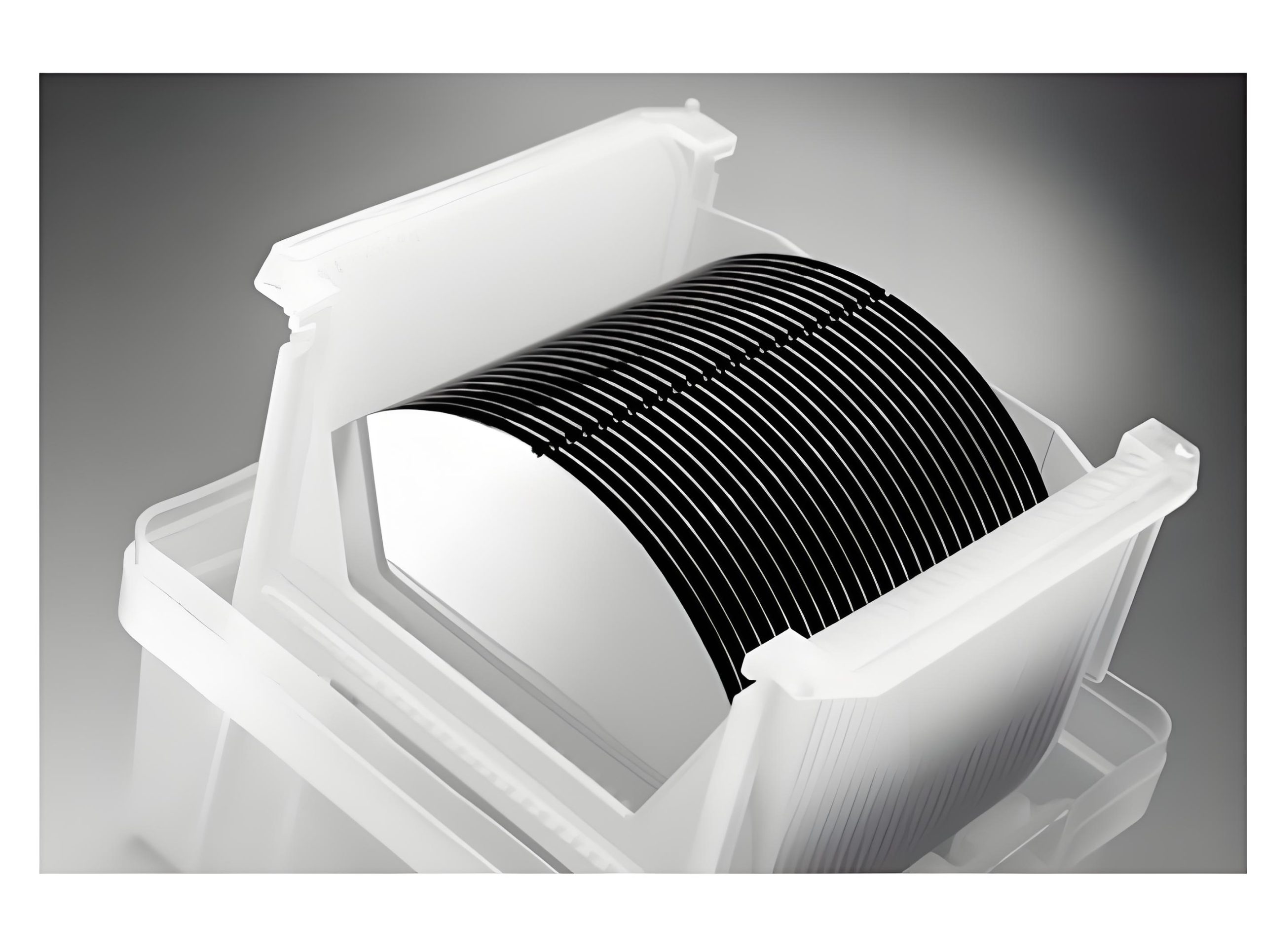
Key Specifications of This 4-Inch FZ Wafer Batch
The complete specifications can be read directly from the product label, organized in the table below:
| Parameter | Specification | Notes |
| Product type | Single-side polished (SSP) | One mirror-polished face, one acid-etched face; suitable for epitaxy and oxidation |
| Diameter | 100 ± 0.2 mm (4 inch) | Tightly controlled tolerance, compatible with standard 4-inch equipment fixtures |
| Growth method | FZ (float zone) | Low oxygen, high purity, high resistivity |
| Orientation | <100> | Mainstream process orientation, compatible with MOS devices and MEMS wet etching |
| Thickness | 525 ± 15 μm | Standard 4-inch thickness, balancing mechanical strength and cost |
| Resistivity | >20,000 Ω·cm | Ultra-high resistivity for RF, detector, and power device substrates |
| Packing | 25 wafers per box | Vacuum-sealed aluminum foil bag with cushioning foam, cleanroom packaging |
Why Every Parameter on the Label Matters
Diameter tolerance ±0.2 mm
Do not underestimate those 0.2 mm. Diameter tolerance directly affects compatibility with wafer auto-handlers, graphite rings, and chucks. Out-of-tolerance wafers can jam during transfer or even break — a point especially worth attention for small-volume research orders.
Thickness 525 ± 15 μm
The industrial standard thickness for 4-inch wafers is 500–525 μm. A ±15 μm tolerance represents the mainstream industry level and ensures consistency in subsequent thinning and bonding processes.
Orientation <100>
The <100> orientation is the most widely used for silicon MOS devices and MEMS processes. During anisotropic wet etching (KOH, TMAH), it produces well-defined 54.7° sloped sidewalls — a classic choice for sensor fabrication.
Typical Applications of High-Resistivity FZ Wafers
RF and Microwave Devices
In RF switches, LNAs, and thin-film bulk acoustic resonator (FBAR) filter substrates, high-resistivity substrates minimize eddy-current losses in the substrate, significantly improving insertion loss and linearity. At 20 kΩ·cm and above, substrate conduction losses are essentially eliminated.
Power Devices
Punch-through power devices such as IGBTs and fast-recovery diodes commonly use FZ substrates. With low oxygen content, FZ wafers avoid parameter drift caused by oxygen-donor effects, giving high-voltage devices better voltage-blocking stability.
Radiation Detectors
Silicon PIN detectors and particle detectors require near-intrinsic, high-resistivity substrates to build the depletion region — >20 kΩ·cm is precisely the mainstream specification range for such applications.
MEMS and Scientific Research
Piezoresistive sensors, bulk-silicon etched structures, and process development at universities and research institutes frequently use 4-inch high-resistivity FZ wafers as the standard experimental carrier, and the 25-wafer small-batch packaging matches research workflows perfectly.
FZ vs. CZ High-Resistivity Wafers: Which to Choose?
| Comparison | FZ (Float Zone) | CZ (Czochralski) |
| Oxygen content | Extremely low (<1×10¹⁶ cm⁻³) | Relatively high (about 1×10¹⁸ cm⁻³) |
| Resistivity ceiling | Can exceed 20 kΩ·cm, near intrinsic | High resistivity is difficult to achieve and prone to drift |
| Mechanical strength | Relatively lower | Better (oxygen-strengthened) |
| Cost | Higher | Lower |
| Typical applications | RF, detectors, high-voltage power devices | Integrated circuits, standard discrete devices |
Buying Recommendations
When purchasing high-resistivity FZ wafers, we recommend confirming your requirements in the following order to avoid paying for mismatched specifications:
Define Your Process First, Then Your Specification
Clarify the downstream process route: for epitaxy or thermal oxidation, SSP wafers are sufficient; for double-side thinning or bonding, consider DSP (double-side polished) wafers; for anisotropic wet etching, be sure to confirm the <100> orientation and the primary flat position.
Choose Resistivity to Match Your Application — Not Just the Highest Number
For RF applications, ≥1 kΩ·cm already delivers clear benefits; for detector applications, go directly to the >20 kΩ·cm grade. Higher resistivity means higher cost, so matching the specification to the application is the most cost-effective approach.
Pay Attention to Packaging and Shipping
High-resistivity FZ wafers have lower mechanical strength than CZ wafers, and breakage in transit is a common after-sales issue. This batch ships in vacuum-sealed aluminum foil bags with cushioning foam for moisture and shock protection. Upon receipt, we recommend letting the package rest until it reaches room temperature in a clean environment before opening, to prevent condensation from contaminating the polished surface.
Validate with a Small Batch Before Scaling Up
Research users are advised to start with a 25-wafer small batch for process validation, and discuss volume pricing only after confirming the parameters match — this greatly reduces trial-and-error costs.
Frequently Asked Questions (FAQ)
Q1: How is a resistivity above 20,000 Ω·cm achieved? A: Through the ultra-high purity of the float-zone process itself and minimal dopant residue — the material approaches intrinsic silicon without any compensation doping.
Q2: What is the difference between SSP and DSP wafers, and which should I choose? A: SSP wafers have one mirror-polished face and one acid-etched face, suited to single-sided processes such as epitaxy and oxidation, at a lower price. DSP wafers are mirror-polished on both sides, for applications requiring backside optical measurement or double-sided processes.
Q3: Can 4-inch wafers also be cut into square pieces? A: Yes. Besides standard round wafers, the same FZ silicon material can be cut into squares, strips, and other custom shapes to your drawings, with a slightly longer lead time.
Q4: Any precautions for storing high-resistivity wafers? A: Keep them in the vacuum packaging and store in a nitrogen cabinet or a dry environment (humidity < 40%) to avoid oxidation and contamination of the polished surface. After opening, return unused wafers to a clean wafer carrier and reseal promptly.
Q5: What does the conductivity type in “Type/Orientation: <100>” on the label mean? A: High-resistivity wafers are usually high-resistivity N-type or P-type; refer to the batch COA (Certificate of Analysis) for specifics. Near-intrinsic material has minimal conductivity-type impact on devices, but you may specify it when ordering.
Q6: Why are FZ wafers more expensive than CZ wafers? A: Float-zone growth is slower, demands higher polysilicon rod quality, and is limited in achievable diameter — so the process cost is inherently higher. In return, you get unmatched high-resistivity and low-oxygen performance.
For detailed specifications, COA reports, or custom-size quotations for 4-inch and 6-inch FZ high-resistivity silicon wafers, please contact our sales team.
Single-Crystal Silicon Wafers: The Foundation of Modern Electronics Prime silicon wafer for semiconductor Solar Cells P type N type,2 to 12inch 511晶向单抛硅片怎么选