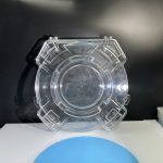
PRODUCTS DETAILS
| Orientation | C-plane<0001> +/- 1 deg. |
| Diameter | 300.0 +/-0.25 mm |
| Thickness | 1.0 +/-25um |
| Notch | Notch or Flat |
| TTV | <50um |
| BOW | <50um |
| Edges | Protactive chamfer |
| Front side – polished 80/50 | |
| Laser mark | None |
| Packaging | Single wafer carrier box |
| Front side Epi ready polished (Ra <0,3nm) | |
| Back side Epi ready polished (Ra <0,3nm) | |
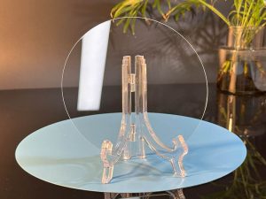
1. Sapphire substrate surfaces have an extremely low particle count, with fewer than 50 particles 0.3 microns or larger per 2 inches in the 2 to 8 inch size range, and major metals (K, Ti, Cr, Mn, Fe, Co, Ni, Cu, Zn) below 2E10/cm2. The 12-inch base material is also expected to achieve this grade. 2. Can be used as a carrier wafer for the 12-inch semiconductor manufacturing process (in-device transport pallets) and as a substrate for bonding. 3. Can control the shape of concave and convex surface. Material: High purity single crystal Al2O3, sapphire wafer. LED quality, no bubbles, cracks, twins, lineage, no color..etc.
4 inch Sapphire Wafer C-Plane SSP/DSP 0.43mm 0.65mm 200mm 8inch GaN on sapphire Epi-layer wafer substrate xinkehui
