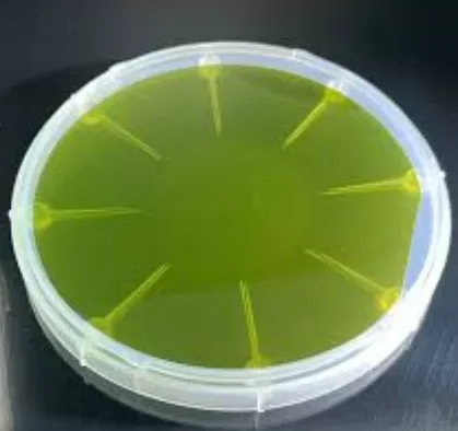
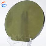
The 8-inch P Grade N-type SiC Substrate is a high-performance silicon carbide crystal substrate designed specifically for demanding power applications. Known for its high conductivity, this 8-inch N-type SiC for power devices provides exceptional thermal management and reliability, making it an ideal choice for high-voltage and high-temperature environments. Engineered as a P Grade 8-inch N-type SiC Wafer, this substrate offers superior purity and precision, ensuring efficient energy handling in critical applications.
Utilized in sectors like electric vehicles and industrial power, this 8-inch Silicon Carbide Power Device Substrate supports robust power conversion systems by maintaining stability even under extreme conditions. Its high purity and N-type conductivity optimize it for power semiconductors, ensuring minimal energy loss and enhanced device longevity. As a P Grade SiC Crystal for electric vehicles, it’s instrumental in reducing power inefficiencies, supporting sustainable energy solutions.
Overall, the P Grade 8-inch N-type SiC Wafer is not only a foundation for next-generation power electronics but also a versatile 8-inch SiC for power semiconductors that addresses the rigorous demands of modern power device applications.
P Grade 8inch N type SiC substrate ‘s specification
| P grade N type SiC Crystal Parameters | |
| Polytype | 4H |
| Polytype Area | None Permitted |
| Micropipe Density | -2 ≤1 cm |
| Hex Plates | None Permitted |
| Hexagonal Polycrystalline | None Permitted |
| Inclusion | area≤0.05% |
| Resistivity | 0.015Ω•cm—0.025Ω•cm |
| EPD | ≤8000 cm-2 |
| TED | ≤6000 cm-2 |
| BPD | ≤2000 cm-2 |
| TSD | ≤1000 cm-2 |
| SF | ≤1% |
| Metal Contamination | (Al, Cr, Fe, Ni, Cu, Zn, Pb, Na, K, Ti, Ca, V, Mn) ≤1E11 cm-2 |
| Mechanical Parameters | |
| Diameter | 200.0 mm+0mm/-0.5mm |
| Surface Orientation | 4°toward <11-20>±0.5° |
| Primary Flat Length | Notch |
| Secondary Flat Length | None |
| Notch Orientation | <1-100>±1° |
| Notch Angle | 90° +5°/-1° |
| Notch Depth | 1mm +0.25mm/-0mm |
| Orthogonal Misorientation | ±5.0° |
| Surface Finish | C-Face: Optical Polish, Si-Face: CMP |
| Wafer Edge | Beveling |
| Surface Roughness (10μm×10μm) |
Si-Face:Ra≤0.2 nm C-Face:Ra≤0.5 nm |
| Thickness | 500.0μm±25.0μm |
| LTV (10mmx10mm) | ≤3μm |
| TTV | ≤10μm |
| BOW | ≤25μm |
| Warp | ≤40μm |
| Surface Parameters | |
| Chips/Indents | None permitted≥0.5mm Width and Depth |
| a Scratches (Si face CS8520) |
≤5 and Cumulative Length≤ 1 Wafer Diameter |
| a TUA (2mm*2mm) |
≥95% |
| Cracks | None Permitted |
| Stain | None Permitted |
| Edge Exclusion | 3mm |
Key Properties of P Grade 8-inch N-type SiC Substrate:
- Size and Dimensions
- Diameter: 8 inches (approximately 200 mm)
- Thickness: Typically around 350 micrometers, with precise control to support consistent manufacturing processes.
- Crystal Type
- Polytype: Available in both 4H-SiC and 6H-SiC configurations, depending on application needs, each offering specific properties in terms of electron mobility and thermal conductivity.
- Doping Type
- N-type: Enhanced with nitrogen doping, ideal for high-power and high-frequency applications.
- Electrical Properties
- High Conductivity: P Grade 8inch N type SiC substrate Exhibits low electrical resistivity, supporting efficient current flow, which is crucial for power devices.
- Breakdown Electric Field: High breakdown voltage, allowing it to withstand high voltages without degrading performance.
- Thermal Properties
- High Thermal Conductivity: Excellent heat dissipation capabilities, ensuring stable operation in high-temperature environments.
- Thermal Expansion Coefficient😛 Grade 8inch N type SiC substrate Low coefficient ensures structural integrity under thermal cycling.
- Purity and Quality Grade
- P Grade: High purity, optimized for research and high-performance applications.
- Micropipe Density: Typically less than 0.5 cm², minimizing defects and improving device longevity.
- Applications
- Ideal for power devices in electric vehicles, renewable energy systems, industrial power supplies, and other high-performance semiconductor applications.
- Mechanical Properties
- High Hardness: P Grade 8inch N type SiC substrate High on the Mohs hardness scale (~9.2), offering durability and resilience in device fabrication and operation.
Advantages
- Superior Reliability in high-stress environments, making it suitable for applications requiring consistent performance under extreme conditions.
- Extended Device Lifespan thanks to low defect rates and robust material integrity.
- Efficiency Boost: Lower energy losses and higher operating efficiency in power conversion systems.
These properties make the P Grade 8-inch N-type SiC substrate a top choice for next-generation power semiconductors, supporting innovations in energy-efficient, high-power electronic devices.
Sapphire window optical elements coated multi-size specifications Optical infrared window 200mm 8inch GaN on sapphire Epi-layer wafer substrate 8Inch 200mm 4H-N SiC Wafer Conductive dummy research grade


