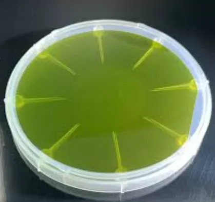
A 6-inch N-type SiC substrate refers to a wafer of silicon carbide (SiC) crystal with specific properties. Here’s a breakdown of its key characteristics and significance:
1. Material: Silicon Carbide (SiC)
-
Wide Bandgap Semiconductor (~3.2 eV for 4H-SiC): Enables high-temperature operation (>200°C), high voltage handling, and high thermal conductivity.
-
High Breakdown Electric Field: ~10× higher than silicon, allowing thinner drift layers and higher power density.
-
Thermal Conductivity: ~3× higher than silicon, improving heat dissipation.
2. Diameter: 6 inches (150 mm)
-
Industry Transition: The shift from 4-inch (100 mm) to 6-inch substrates reduces manufacturing costs by increasing die yield per wafer (~2.25× more area).
-
Adoption Status: Leading manufacturers (Wolfspeed, II-VI, SK Siltron) now mass-produce 6-inch wafers; 8-inch (200 mm) is in R&D/pilot lines.
3. Conductivity Type: N-type
-
Dopant: Typically nitrogen (N), creating free electrons for current conduction.
-
Resistivity: Ranges from 0.01–0.03 Ω·cm (low-resistivity for epitaxy) to ~0.02 Ω·cm (device-ready).
-
Applications: Used as starting material for high-voltage diodes, MOSFETs, JFETs, and RF devices.
4. Polytype: 4H-SiC Dominance
-
Structure: Hexagonal (4H) polytype is standard for power devices due to superior electron mobility and thermal stability over 6H or 3C-SiC.
5. Key Specifications
-
Thickness: 350–500 μm (may be thinned post-fabrication).
-
Micropipe Density (MPD): Historically critical; now < 1 cm⁻² in commercial wafers.
-
Dislocation Defects:
-
Threading Screw Dislocations (TSD): < 500 cm⁻²
-
Basal Plane Dislocations (BPD): < 1,000 cm⁻²
-
-
Surface Finish: Epitaxy-ready with Ra < 0.2 nm (CMP-polished).
6. Applications
-
Power Electronics: EV inverters, fast chargers, industrial motor drives.
-
RF Devices: 5G base stations, radar systems (benefiting from high electron saturation velocity).
-
Harsh Environments: Aerospace, downhole drilling.
7. Market & Supply Chain
-
Key Suppliers: Wolfspeed (Cree), Coherent (II-VI), SK Siltron, STMicroelectronics.
-
Cost Trend: ~$800–$1,200/wafer (declining as yields improve).
-
Challenges: Crystal growth defects, high-energy consumption during production.
Why 6-inch N-type Matters:
-
Cost Reduction: Larger wafers → lower $/die → accelerated adoption in EVs/industrial systems.
-
Performance: Enables 1.2–3.3 kV devices with higher efficiency vs. Si-based solutions.
| Properties | Specification | Unit | ||||
| Z | P | R | D | |||
| Diameter | 150± 0.25 | mm | ||||
| Thickness | 350(-25, 25) | µm | ||||
| Surface off-orientation | 4.0° towards [11-20]± 0.5° | |||||
| Primary flat location | Perpendicular to the [11-20]± 5° | |||||
| Primary flat length | 47.5 ± 1.5 | mm | ||||
| Edge Exclusion | 3 | mm | ||||
| Warp | ≤ 25 | ≤ 35 | ≤ 45 | ≤ 60 | µm | |
| Bow | ± 10 | ± 15 | ± 25 | ± 40 | µm | |
| TTV | ≤ 5 | ≤ 8 | ≤ 10 | ≤ 15 | µm | |
| Dislocation Density-EPD | ≤ 4000 | ≤ 6000 | ≤ 8000 | ≤ 12000 | No
requirements |
/cm2 |
| Dislocation Density-TSD | ≤ 200 | ≤ 300 | ≤ 500 | ≤ 800 | /cm2 | |
| Dislocation Density-BPD | ≤ 800 | ≤ 1000 | ≤ 1500 | ≤ 2000 | /cm2 | |
| Micropipe Density | ≤ 0.2 | ≤ 0.2 | ≤ 0.5 | ≤ 1 | /cm2 | |
| Polytype by high intensity
light |
4H 100% | 4H 98% | 4H 97% | % area | ||
| Hexagon by high intensity
light |
None | ≤1% | ≤3% | % area | ||
| Resistivity | 0.015-0.025 | 0.015-0.028 | 0.010-0.030 | Ω·cm | ||
| Surface roughness( Si face) | < 0.2 | nm | ||||
| Surface roughness( C face) | < 1 | < 2 | nm | |||
| Cracks by high intensity light | none | |||||
| Si surface scratches by high intensity light | none | ≤3ea ,each ≤ 10mm | ||||
| Cumulative scratches length
(By 8520) |
≤ 75 | ≤ 100 | ≤150 | No requirements | mm | |
| Edge chip | none | |||||
| Edge Profile | SEMI M55-0817 | |||||
| Stains by high intensity light | none | |||||
| Residual Metals
Contamination (Al, Cr, Fe, Ni, Cu, K, Ti &Mn) |
< 5E10 | < 1E11 | ||||
| Packaging | Multi-wafer Cassette/Single-wafer box | |||||
Sic Wafer Silicon Wafer 4H-N/Semi Type SiC Ingots Industrial 6inch 150mm Silicon Carbide SiC Wafers 4H-N type for MOS or SBD Production Research and Dummy grade 8Inch 200mm 4H-N SiC Wafer Conductive dummy research grade 6inch sic substrate 2inch 50.8mm Germanium Wafer Substrate Single crystal 1SP 2SP 200mm 8inch GaN on sapphire Epi-layer wafer substrate


