一、Introduction to ALN Ceramic Substrates
ALN ceramic substrates have emerged as critical materials in modern electronic applications where efficient heat dissipation and reliable performance are paramount. These advanced substrates, composed of aluminum nitride (AlN), offer an exceptional combination of high thermal conductivity, excellent electrical insulation, and remarkable mechanical properties that make them indispensable in high-power and high-frequency electronic devices .
The significance of ALN substrates lies in their ability to address one of the most pressing challenges in contemporary electronics: thermal management. As electronic devices become increasingly powerful and compact, effective heat dissipation becomes crucial for maintaining performance, reliability, and longevity. ALN ceramic substrates provide an optimal solution, with thermal conductivity ranging from 170-230 W/(m·K), far surpassing traditional alumina substrates .
What sets ALN substrates apart is not just their impressive thermal properties but also their coefficient of thermal expansion (CTE), which closely matches that of silicon (approximately 4.5 ppm/℃). This compatibility minimizes thermal stress at critical interfaces between chips and substrates, significantly enhancing the reliability of semiconductor devices .
The evolution of ALN technology represents a milestone in materials science, offering a non-toxic alternative to beryllium oxide (BeO), which was previously used for high thermal conductivity applications but raised health and environmental concerns . This advantage, combined with ongoing manufacturing advancements, has positioned ALN as the material of choice for demanding applications across various high-tech industries.
二、Key Properties and Advantages of ALN Substrates
Exceptional Thermal Management Capabilities
The most distinguished property of ALN ceramic substrates is their outstanding thermal conductivity, which typically ranges between 170-230 W/(m·K) . This remarkable capability enables ALN substrates to efficiently transfer heat away from sensitive electronic components, preventing overheating and ensuring optimal performance. The thermal management efficiency of ALN is approximately 5-10 times greater than that of conventional aluminum oxide (Al₂O₃) substrates, making ALN indispensable for high-power applications .
The thermal performance of ALN stems from its unique crystal structure and high purity. Achieving optimal thermal conductivity requires precise control during manufacturing, as even minimal oxygen contamination can significantly reduce this property. Advanced sintering techniques have enabled manufacturers to produce ALN substrates with consistently high thermal performance, meeting the rigorous demands of modern electronic applications .
Optimal Electrical and Mechanical Properties
Beyond thermal management, ALN substrates offer excellent electrical insulation properties, with volume resistivity typically exceeding 10¹³ Ω·cm and dielectric strength of 25 kV/mm or higher . These characteristics make ALN substrates ideal for high-voltage applications where reliable insulation is critical for safety and performance.
The dielectric properties of ALN are equally impressive, with a relatively low dielectric constant (8-10 at 1 MHz) and minimal dielectric loss (tan δ ≈ 0.0005) . These properties ensure minimal signal distortion and loss in high-frequency applications, which is particularly important for RF and microwave circuits where signal integrity is paramount.
Mechanically, ALN substrates demonstrate superior strength with flexural strength typically exceeding 450 MPa, substantially higher than many alternative ceramic materials . This mechanical robustness ensures that ALN substrates can withstand the rigors of manufacturing processes and operational environments without cracking or degrading, providing long-term reliability for critical electronic systems.
Material Compatibility and Stability
The thermal expansion coefficient of ALN (approximately 4.3×10⁻⁶/°C) closely matches that of silicon (3.5-4.0×10⁻⁶/°C), a critical advantage for semiconductor applications . This compatibility minimizes thermal stress at the silicon-Ceramic interface during temperature cycling, reducing the risk of delamination, cracking, or other failure mechanisms that can compromise device reliability.
ALN substrates also exhibit exceptional chemical stability, resisting degradation from most chemicals and maintaining performance in harsh environments. This stability, combined with their non-toxic composition, makes ALN an environmentally preferable choice compared to alternatives like beryllium oxide .
Comparison of Key Properties of Ceramic Substrate Materials
| Property | ALN (Aluminum Nitride) | Al₂O₃ (Alumina) | BeO (Beryllia) |
|---|---|---|---|
| Thermal Conductivity (W/m·K) | 170-230 | 20-30 | 330 |
| CTE (×10⁻⁶/°C) | 4.3 | 7.2 | 7.5 |
| Dielectric Constant | 8.5-9.5 | 9.8 | 7.0 |
| Flexural Strength (MPa) | >450 | 300-400 | 200-250 |
| Toxicity | Non-toxic | Non-toxic | Highly toxic |
三、Major Applications of ALN Ceramic Substrates
Power Electronics and Automotive Systems
In the realm of power electronics, ALN substrates have become essential components for insulated gate bipolar transistors (IGBTs), power MOSFETs, and other high-power semiconductor devices. The exceptional thermal management capabilities of ALN enable these devices to operate at higher power densities and temperatures while maintaining reliability . This advantage is particularly valuable in electric vehicle systems, where power conversion modules, motor drives, and charging infrastructure benefit from ALN’s ability to handle high thermal loads in compact form factors.
The automotive industry’s rapid shift toward electrification has significantly increased demand for ALN substrates. In these applications, ALN substrates serve as the foundation for power modules that control traction motors, manage battery systems, and facilitate rapid charging. The reliability offered by ALN is critical for meeting automotive safety standards and warranty requirements, as failure of these components can have serious consequences .
LED and Optoelectronic Devices
High-brightness LED systems represent another major application area for ALN substrates. The high efficiency of modern LEDs comes with significant heat generation that must be effectively managed to maintain light output, color stability, and operational life. ALN substrates provide the thermal pathway necessary to keep junction temperatures within safe limits, enabling the development of brighter, more compact, and longer-lasting LED systems .
In specialized optoelectronic applications such as laser diodes and optical communication modules, ALN substrates offer the combination of thermal management, electrical isolation, and high-frequency performance required for reliable operation. The dimensional stability of ALN under thermal cycling ensures precise alignment of optical components, which is critical for maintaining performance in fiber optic communication systems and precision laser applications .
RF/Microwave and Aerospace Applications
The telecommunications industry relies on ALN substrates for 5G infrastructure, radar systems, and satellite communications where high-frequency performance and thermal management are simultaneously required. ALN’s low dielectric loss makes it suitable for high-frequency circuits, while its thermal conductivity manages heat generated by power amplifiers and other active components .
In aerospace and defense applications, ALN substrates provide the reliability needed for critical systems that must operate in extreme environments. The combination of thermal stability, resistance to thermal shock, and consistent high-frequency performance makes ALN the material of choice for phased array radars, electronic warfare systems, and avionics where failure is not an option .
Emerging and Specialty Applications
As technology advances, new applications for ALN substrates continue to emerge. In medical electronics, ALN substrates enable the development of more powerful and compact medical imaging systems, therapeutic devices, and implantable electronics where reliability and thermal management are critical. The renewable energy sector utilizes ALN in power conversion systems for solar and wind energy installations, where efficient thermal management directly impacts energy conversion efficiency and system longevity .
The growing field of wide bandgap semiconductors (SiC and GaN) has further increased the importance of ALN substrates. These semiconductor materials operate at higher temperatures, frequencies, and power densities than traditional silicon, creating thermal management challenges that ALN is uniquely positioned to address .
四、Technical Specifications: Sizes, Dimensions, and Manufacturing Standards
Standard Size Offerings and Customization
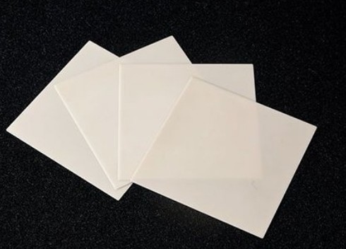
A common question among those considering ALN ceramic substrate purchase is regarding available sizes. The maximum size of ALN ceramic substrates has increased with manufacturing advancements, with standard panel sizes typically ranging from 4.5×4.5 inches to 5.5×7.5 inches . For specialized applications, manufacturers can produce larger formats, with some capable of fabricating substrates up to 175×175 mm (approximately 6.9×6.9 inches) .
The available thickness options for ALN substrates typically range from 0.25 mm to 3.0 mm, with 0.635 mm being a common standard thickness that provides an optimal balance between mechanical strength, thermal performance, and weight considerations . Manufacturers can produce custom dimensions to meet specific application requirements, though non-standard sizes may impact lead times and cost.
Manufacturing Processes and Quality Standards
The production of ALN substrates involves sophisticated manufacturing techniques including tape casting, high-temperature sintering in controlled atmospheres, and precision machining to achieve tight tolerances. HTCC (High-Temperature Co-fired Ceramic) is a common manufacturing approach for multilayer ALN substrates, requiring sintering temperatures above 1600°C . This process necessitates the use of refractory metals such as tungsten or molybdenum for conductive pathways, as conventional silver or gold conductors cannot withstand these extreme temperatures .
Quality control is paramount in ALN substrate production, with manufacturers implementing rigorous inspection protocols to ensure dimensional accuracy, surface finish quality, and material purity. Standard specifications include surface roughness typically between 0.2-0.6 μm, flatness within 2‰ of the longest dimension, and precise control of mechanical properties to ensure consistent performance .
五、Critical Considerations for ALN Ceramic Substrate Purchase
Material Selection Parameters
When planning an ALN ceramic substrate purchase, several technical parameters should guide your selection process. The thermal conductivity requirement should be the primary consideration, with most commercial ALN substrates offering 170-230 W/(m·K). Applications involving high power densities or extreme environments may justify premium-grade materials with thermal conductivity at the upper end of this range .
The dielectric properties should align with your application’s frequency requirements. For high-frequency circuits, substrates with lower dielectric constants (closer to 8.5) are preferable to minimize signal propagation delays. The coefficient of thermal expansion matching to your semiconductor materials is another critical factor, particularly for applications involving large temperature variations or direct chip attachment .
Supplier Evaluation and Quality Assurance
Selecting a reliable manufacturer is as important as specifying the right material properties. When evaluating potential suppliers for your ALN substrate purchase, consider their manufacturing capabilities, quality control processes, and technical support offerings. Established manufacturers with vertical integration—controlling the process from powder production to finished substrate—typically deliver more consistent quality and better technical support .
Reputable suppliers should provide comprehensive certification including material composition analysis, dimensional verification, and performance testing results. For critical applications, additional testing such as thermal cycling validation, bond strength measurements, and microsection analysis may be warranted to ensure the substrates will perform reliably in your specific application .
Cost Considerations and Value Analysis
While ALN substrates command a premium price compared to alumina alternatives—typically 3-5 times higher on a per-unit-area basis—the value proposition extends beyond initial cost . The enhanced performance, reliability, and system-level benefits often justify the investment, particularly in applications where failure carries significant consequences or where performance margins are critical.
When evaluating cost, consider the total system impact including potential savings from simplified thermal management, increased power density, improved reliability, and extended product lifetime. For volume applications, engaging with manufacturers early in the design process can identify opportunities to optimize the substrate design for cost-effective production without compromising performance .
六、ALN Substrate Manufacturing Processes and Technological Advances
Primary Production Techniques
The manufacturing of ALN ceramic substrates involves sophisticated processes that have evolved significantly to meet increasing quality and performance demands. The HTCC (High-Temperature Co-fired Ceramic) process represents a fundamental approach, involving the sintering of ALN green tapes at temperatures exceeding 1600°C . This method enables the creation of complex multilayer structures with embedded conductors, though it requires refractory metals like tungsten or molybdenum for metallization due to the extreme temperatures involved .
Alternative approaches such as DPC (Direct Plated Copper) have gained prominence for applications requiring finer feature resolution. The DPC process involves direct metallization of the ALN substrate through sputtering and plating techniques, enabling higher circuit density and more precise feature definition compared to traditional thick-film approaches . This makes DP


