1. What Are Single-Crystal Silicon Wafers?
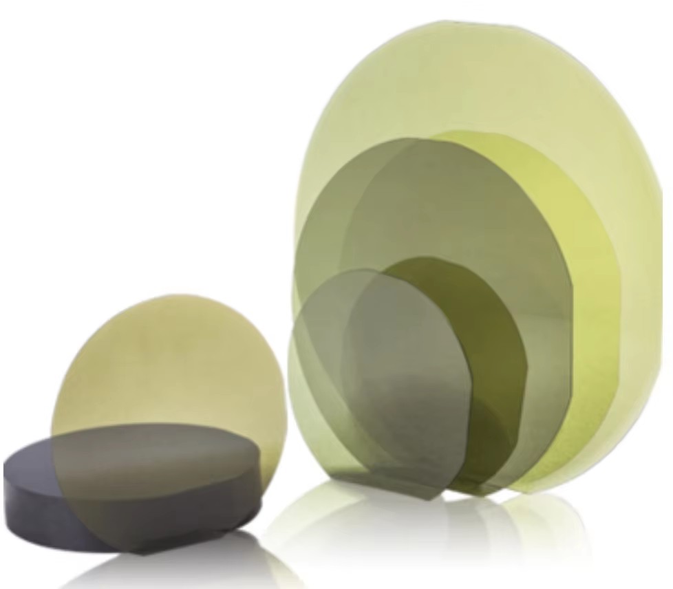
Single-crystal silicon wafers represent the fundamental building blocks of the modern electronics industry. These wafers consist of high-purity silicon arranged in a continuous, unbroken crystal lattice structure with virtually no grain boundaries. This perfect crystalline arrangement gives them superior electronic properties compared to polycrystalline or amorphous silicon materials.
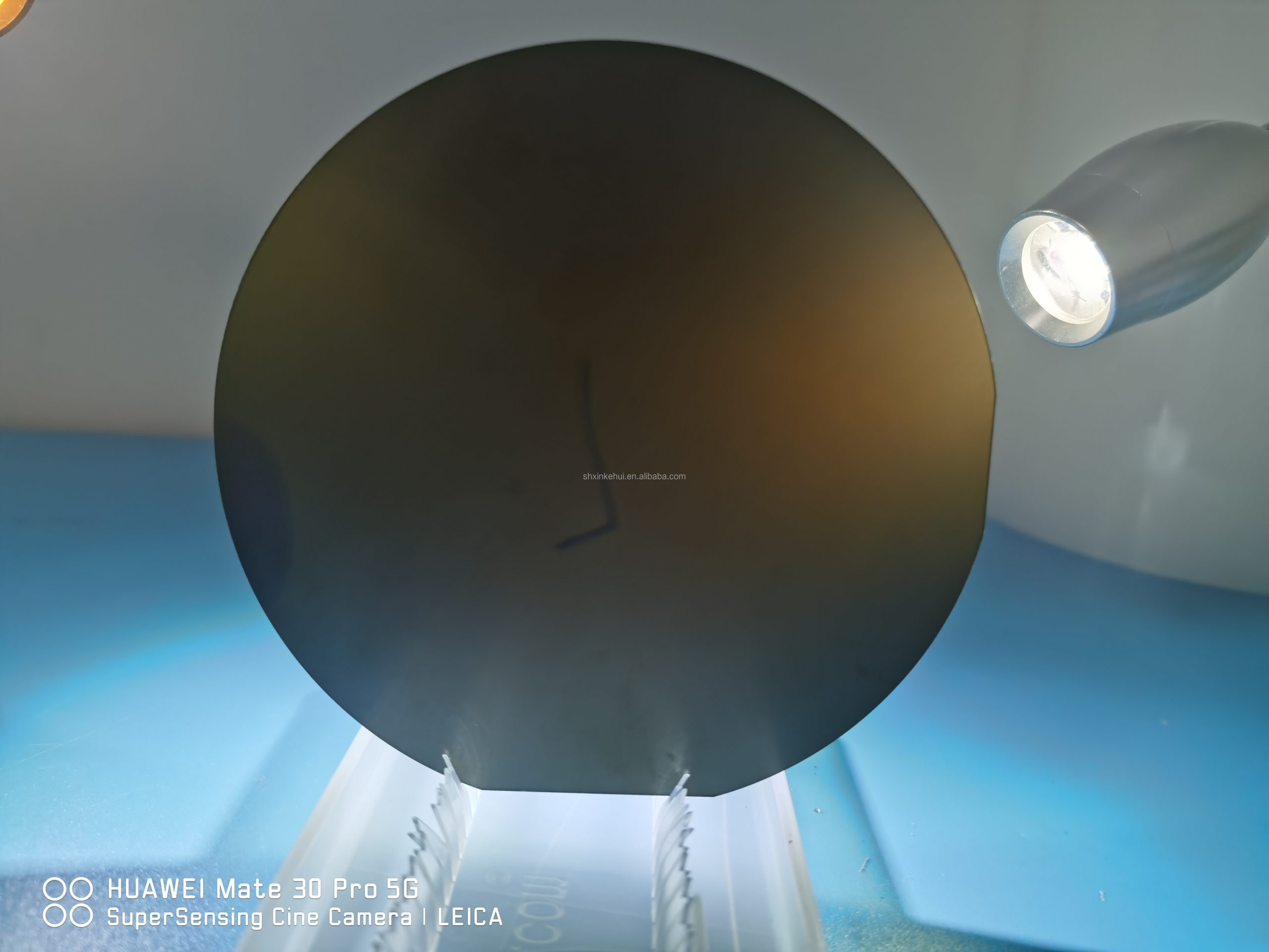
The production of these wafers begins with the Czochralski process, where a seed crystal is slowly pulled from molten silicon, allowing a single crystal to grow . The resulting crystal ingot is then sliced into thin wafers typically measuring between 150-200mm in diameter, though larger 300mm wafers are increasingly common in advanced semiconductor manufacturing. The wafers are polished to a mirror-like finish with surface roughness values as low as 0.075μm achieved through advanced processes like laser grinding .
Single-crystal silicon’s dominance in electronics stems from its semiconductor properties, which can be precisely controlled through doping with specific impurities. The absence of grain boundaries in single-crystal silicon allows for better control of electrical properties and higher charge carrier mobility, making it ideal for high-performance electronic devices . These wafers serve as the substrate for virtually all integrated circuits, microprocessors, and memory chips that power today’s digital world.
2. Key Performance Parameters of Single-Crystal Silicon Wafers
The quality and performance of single-crystal silicon wafers are characterized by several critical parameters that determine their suitability for various applications. The table below summarizes these essential specifications:
| Parameter | Typical Values/Ranges | Significance | Measurement Methods |
|---|---|---|---|
| Purity Level | ≥99.9999% (6N) | Determines electrical properties and device performance | Mass spectrometry, glow discharge mass spectrometry (GDMS) |
| Crystal Orientation | <100>, <111>, <110> | Affects etching characteristics and electronic properties | X-ray diffraction (XRD) |
| Surface Flatness | ≤1μm | Critical for photolithography precision | Laser scanning confocal microscopy |
| Thickness Tolerance | ±5μm or better | Ensures uniformity in manufacturing processes | Precision thickness gauges |
| Oxygen Content | <10 ppma (FZ method) | Affects mechanical strength and electrical properties | Fourier-transform infrared spectroscopy (FTIR) |
| Resistivity | 0.001-100 Ω·cm | Determines electrical conductivity characteristics | Four-point probe measurement |
| Surface Roughness | <0.1μm (after polishing) | Impacts layer deposition quality | Atomic force microscopy, profilometry |
The crystal orientation is particularly important as it influences how the wafer behaves during etching processes and affects the electronic properties of the final devices. Wafers with <100> orientation are most common for metal-oxide-semiconductor (MOS) devices, while <111> orientation is often used for bipolar junctions .
The exceptional surface flatness (typically ≤1μm) enables the extremely fine patterns required in modern photolithography processes, where features smaller than 10nm must be accurately defined . The resistivity of the wafer, which can be precisely controlled through doping, ranges from 0.001 to 100 Ω·cm depending on the intended application, with lower resistivity preferred for power devices and higher resistivity suitable for high-frequency applications .
3. Manufacturing Processes and Technological Advances
The production of single-crystal silicon wafers has evolved significantly, with two primary methods dominating the industry: the Czochralski (CZ) process and the Float Zone (FZ) technique.
3.1 Czochralski Process
The Czochralski method is the most widely used approach for commercial wafer production. This process involves pulling a seed crystal from molten silicon contained in a quartz crucible. The method produces large-diameter crystals (up to 300mm) suitable for mass production of integrated circuits. However, the contact with the quartz crucible introduces oxygen impurities (typically 10-20 ppma) into the crystal, which can affect device performance in some high-frequency applications .
Recent advancements in CZ technology have focused on reducing oxygen content and improving crystal uniformity. The development of magnetic Czochralski (MCZ) method, which applies a magnetic field to control melt convection, has significantly reduced oxygen incorporation and improved dopant uniformity .
3.2 Float Zone Method
The Float Zone technique produces higher-purity silicon with significantly lower oxygen content (<1 ppma) compared to CZ silicon. In this method, a polycrystalline silicon rod is passed through a localized molten zone, which moves along the rod, leaving behind a single crystal. The FZ method is crucible-free, eliminating the primary source of oxygen contamination .
The exceptional purity of FZ silicon wafers makes them ideal for high-power devices and applications requiring high breakdown voltages. However, the method is more challenging for large-diameter wafers, with 200mm being the current practical limit for commercial production .
3.3 Emerging Methods
The Floating Silicon Method (FSM) represents an innovative approach that directly produces single-crystal ribbons or wafers from a silicon melt. This technique grows crystals in a horizontal configuration, resulting in thin silicon ribbons (as thin as 200μm) with minimal material waste compared to traditional sawing processes. FSM technology promises up to 50% reduction in manufacturing costs and 56% reduction in manufacturing emissions compared to conventional CZ processing .
Laser grinding has emerged as a promising surface finishing technique that significantly improves surface quality. Research shows that laser grinding can reduce surface roughness from 400nm to 75nm while efficiently removing the SiO₂ layer derived from mechanical machining processes .
4. Applications Across Industries
Single-crystal silicon wafers serve as the foundation for numerous electronic and optoelectronic devices that are essential to modern technology.
4.1 Integrated Circuits and Microprocessors
The most significant application of single-crystal silicon wafers is in the fabrication of integrated circuits (ICs) and microprocessors. The excellent semiconductor properties of silicon, combined with the thermal stability of single-crystal wafers, enable the creation of billions of transistors on a single chip. The continuous scaling of ICs to smaller feature sizes (now approaching 3nm) has been possible due to improvements in wafer quality and purity .
4.2 Solar Cells and Photovoltaics
In the renewable energy sector, single-crystal silicon wafers are used to produce high-efficiency solar cells. While polycrystalline silicon dominates the lower-cost segment of the solar market, single-crystal silicon solar cells achieve the highest conversion efficiencies, exceeding 24% in commercial production . The superior crystal quality minimizes charge carrier recombination, leading to better performance, especially in space applications and concentrated photovoltaic systems .
Advanced surface texturing techniques, such as the creation of inverted pyramid structures through metal-assisted chemical etching, have further improved light trapping in solar cells, reducing surface reflectance to as low as 4.6% .
4.3 Sensors and MEMS
Single-crystal silicon wafers are the substrate of choice for microelectromechanical systems (MEMS) and various sensors. The excellent mechanical properties of silicon, combined with its well-established fabrication processes, make it ideal for creating miniature mechanical structures. Applications include accelerometers in airbags, gyroscopes in smartphones, pressure sensors, and optical mirrors .
4.4 Power Devices
For high-power applications, such as those in electric vehicles and power grids, single-crystal silicon wafers with specific resistivity characteristics are essential. Float-zone silicon is particularly valuable for these applications due to its high purity and ability to handle high voltages and currents efficiently .
5. Future Perspectives and Challenges
The single-crystal silicon wafer industry continues to evolve to meet the demanding requirements of next-generation electronic devices.
The trend toward larger wafer diameters continues, with 450mm wafers in development, though their commercial implementation faces significant technical and economic challenges. Larger wafers improve manufacturing efficiency but require substantial equipment upgrades and present greater challenges in maintaining uniformity .
Researchers are exploring alternative crystal growth techniques that could reduce costs and environmental impact. The Floating Silicon Method shows particular promise for solar applications, potentially reducing silicon waste by over 50% compared to conventional sawing processes .
Defect engineering has become increasingly important as feature sizes shrink. Advanced characterization techniques, including resonance ultrasonic vibration and laser-based thermography, are being developed for rapid, non-destructive detection of micro-cracks and other defects that can affect device yield and reliability .
The development of silicon-on-insulator (SOI) wafers, which incorporate a buried oxide layer, addresses performance issues in advanced CMOS devices by reducing parasitic capacitance and improving radiation hardness. While more expensive than conventional wafers, SOI technology is finding increasing application in high-performance and specialized computing.
As the Internet of Things (IoT) and artificial intelligence (AI) drive demand for more computing power, single-crystal silicon wafers will continue to be the foundation of electronic innovation, with ongoing improvements in quality, diameter, and cost-effectiveness shaping the future of the semiconductor industry.
6. Conclusion
Single-crystal silicon wafers represent one of the most technologically significant materials developed in the past century. Their exceptional purity, perfect crystal structure, and controllable electrical properties have enabled the digital revolution that defines modern society. While alternative semiconductors like gallium arsenide and silicon carbide offer advantages for specific applications, silicon’s abundance, well-established processing technology, and excellent overall properties ensure its continued dominance in mainstream electronics.
As research continues to improve manufacturing techniques, reduce costs, and enhance material properties, single-crystal silicon wafers will remain the bedrock of the electronics industry, supporting continued advancement in computing, communications, renewable energy, and countless other technologies that shape our world.
