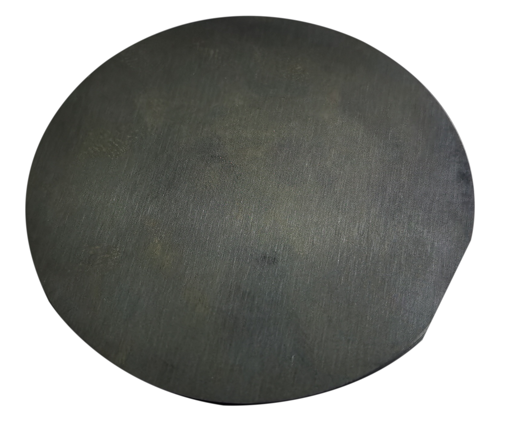
The cost disparity between Silicon-On-Insulator (SOI) wafers and traditional bulk silicon wafers is a critical factor in their adoption across semiconductor industries. While SOI wafers dominate high-performance applications, bulk silicon remains prevalent in cost-sensitive markets. This analysis compares their pricing, manufacturing complexity, yield rates, and application-specific cost-effectiveness.
1. Base Material Costs: SOI Wafers Command a Premium
SOI wafers inherently cost more due to their multi-layer structure (silicon-insulator-silicon) and advanced fabrication processes like Smart Cut™ and SIMOX. As of 2025:
- 200mm SOI wafers: 150 per unit
- 300mm SOI wafers: 500 per unit
- Bulk silicon wafers: 50 (200mm) and 120 (300mm)
The price gap stems from SOI’s ion implantation, wafer bonding, and annealing steps, which add 30–40% to manufacturing costs compared to bulk silicon’s straightforward slicing and polishing .
2. Process Complexity: SOI Reduces Steps but Increases Equipment Costs
While SOI simplifies lithography by minimizing parasitic capacitance, its production involves specialized tools:
- Key SOI Processes:
- Hydrogen ion implantation (10–50 keV)
- High-temperature annealing (1300–1350°C)
- Low-temperature wafer bonding
- Bulk Silicon Processes:
- Czochralski (CZ) or float-zone (FZ) silicon growth
- Standard CMP polishing
SOI’s Smart Cut™ equipment costs 50 million for bulk silicon’s CMP tools . However, SOI eliminates deep reactive ion etching (DRIE) steps for RF components, saving 20–30% in process time .
3. Yield Rates: Bulk Silicon Dominates in Mass Production
| Parameter | Bulk Silicon | SOI Wafers |
|---|---|---|
| 200mm Yield Rate | 85–90% | 65–70% |
| 300mm Yield Rate | 80–85% | 55–60% |
SOI’s lower yields arise from insulator layer defects (e.g., voids in buried oxide) and wafer warpage during thermal processing. Bulk silicon’s mature processes achieve >90% yield for mature nodes (28nm+) .
4. Application-Specific Cost-Benefit Analysis
High-Frequency RF Circuits
- SOI Advantage:
- 50% lower insertion loss in 28GHz filters
- 40% reduction in matching circuit area
- Cost Impact:
- RF front-end modules (FEMs) using SOI save $15–20% in BOM costs despite higher wafer prices .
Automotive Electronics
- SOI Benefit:
- 175°C operational stability (vs. 150°C for bulk silicon)
- 70% lower leakage current in LiDAR drivers
- Cost Impact:
- EV inverter systems using SOI reduce thermal management costs by 12–15% .
IoT and Wearables
- SOI Benefit:
- 40% lower active power consumption
- 30% smaller footprint for motion sensors
- Cost Impact:
- Smartwatch SoCs on SOI save 0.80 per unit in battery costs .
5. Regional Pricing Dynamics and Geopolitical Factors
- Asia-Pacific:
- Dominates SOI production (75% of global capacity)
- Subsidies like China’s “Big Fund” reduce SOI costs by 10–15%
- North America:
- CHIPS Act incentives boost 300mm SOI capacity but increase bulk silicon tariffs by 25%
- Europe:
- CBAM mechanism raises non-EU SOI imports by 6–9%
Export controls on advanced equipment (e.g., ASML’s EUV lithography) delay SOI adoption in China, forcing reliance on older 200mm bulk silicon nodes .
6. Future Trends: Cost Parity Through Innovation
- 3D SOI Integration:
- Stacking SOI wafers reduces interconnect lengths, cutting costs by 20–25%
- Material Innovations:
- High-resistivity SOI (HR-SOI) for RF applications lowers defect density to <0.05/cm²
- Recycling Initiatives:
- 40% of SOI wafers in Japan now use recycled silicon, cutting raw material costs by 18%
Conclusion: Strategic Adoption Based on Application Needs
While bulk silicon remains cost-optimal for mature-node devices, SOI wafers provide unmatched performance in high-frequency, low-power, and high-reliability applications. Manufacturers must weigh:
- Upfront material costs vs. long-term performance gains
- Yield trade-offs against design flexibility
- Regional supply chain risks vs. technological advantages
For 5G, automotive, and IoT applications, SOI’s premium pricing is justified by its system-level savings and performance leadership. As 22nm FD-SOI enters mass production, cost parity with bulk silicon is projected by 2028 .
Final Recommendation:
- Adopt SOI for RF, automotive, and AI edge devices.
- Use bulk silicon for cost-sensitive, high-volume logic chips.
This strategic balance ensures optimal cost-performance ratios across evolving semiconductor landscapes.
C-SOI Wafer-Top Product Recommendations for 2025 BSOI Wafers–for 2025 Sapphire Substrate/wafer for Customizable Dimensions c-plane、a-plane 2inch 3 inch 4 inch


