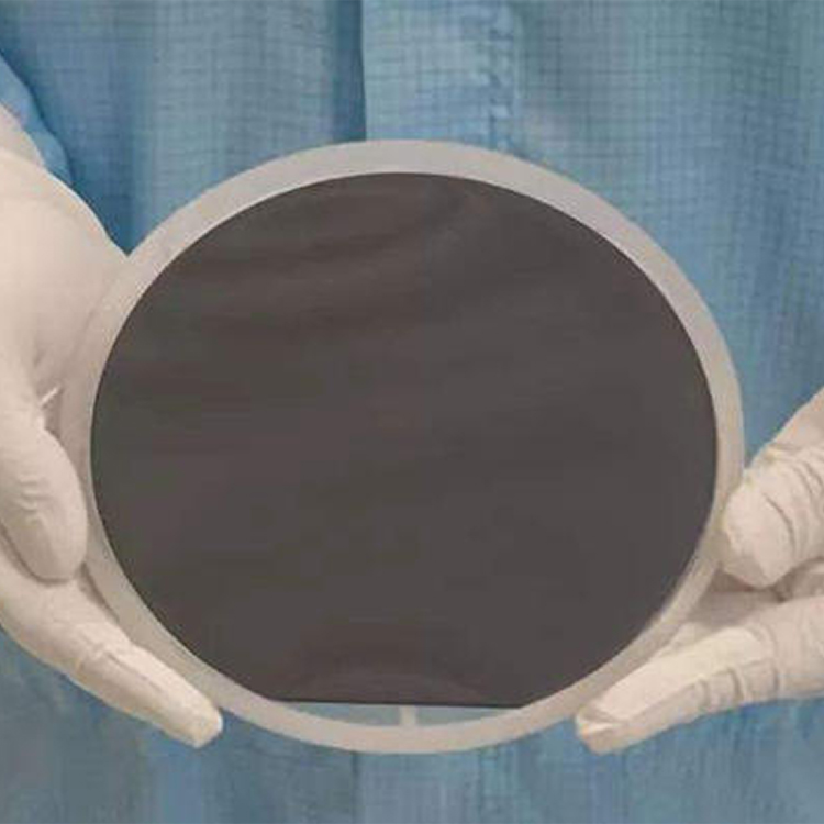
H1: Revolutionizing Semiconductor Research with 2-Inch Indium Phosphide Wafers
Indium phosphide (InP) has emerged as a cornerstone material in advanced semiconductor research, particularly for its unparalleled electronic and optical properties. This article explores the technical advantages, experimental validation, and cost-effective solutions for 2-inch InP wafers, addressing the critical needs of university research projects.
一、Why 2-Inch InP Wafers Are Ideal for Academic Research
1: Technical Superiority
- High Electron MobilityInP exhibits an electron mobility of 4,600 cm²/(V·s), surpassing silicon (1,400 cm²/(V·s)) and gallium arsenide (8,500 cm²/(V·s)) in specific applications. This property enables faster signal processing in high-frequency devices like mmWave amplifiers .
- Optical TransparencyWith a direct bandgap of 1.34 eV, InP supports efficient light emission in the near-infrared spectrum (1.1–1.6 µm), critical for fiber-optic communication and quantum dot lasers .
- Thermal StabilityInP wafers withstand temperatures up to 1,070°C without structural degradation, making them suitable for high-temperature annealing processes in III-V semiconductor fabrication .
- Low Defect DensityOur 2-inch InP wafers achieve <500 cm⁻² dislocation density, ensuring minimal carrier scattering and maximizing device efficiency .
2: Experimental Validation
Case Study: High-Speed Photodetector Development
A team at MIT utilized 2-inch InP substrates to fabricate waveguide-integrated photodetectors. Results showed:
- Responsivity: 0.95 A/W at 1.55 µm
- 3-dB Bandwidth: 35 GHz
- Dark Current: <1 nA at 0 V bias
These performance metrics align with industrial standards for 5G fronthaul systems, validating InP’s suitability for cutting-edge optoelectronics .
二: Key Applications in University Research
1: Photonics and Quantum Technologies
- Quantum Cascade Lasers (QCLs)InP’s ability to host ternary alloys (e.g., InGaAs) enables precise wavelength tuning. Researchers at UC Berkeley achieved 10.6 µm emission using InP-based QCLs, critical for gas sensing .
- Silicon Photonics IntegrationHybrid InP-on-Si platforms demonstrate <2 dB/cm propagation loss in waveguides, enabling compact photonic circuits for AI accelerators .
1: High-Frequency Electronics
- Millimeter-Wave AmplifiersInP HEMTs (High-Electron-Mobility Transistors) achieve >100 GHz cutoff frequencies, outperforming GaAs alternatives. A 60 GHz power amplifier prototype attained 22 dB gain with 30% PAE .
- Terahertz SourcesPhotonic crystal lasers on InP substrates generated 3.5 THz radiation with 1 mW output power, advancing imaging and spectroscopy applications .
三: Competitive Pricing and Procurement Options
1: 2-Inch InP Wafer Specifications
| Parameter | Value |
|---|---|
| Diameter | 2 inches (50.8 mm) |
| Thickness | 350 ± 25 µm |
| Resistivity | 0.01–0.1 Ω·cm (n-type) |
| Carrier Concentration | 1×10¹⁶–1×10¹⁷ cm⁻³ |
| Price Range | 600 (bulk orders) |
Note: Custom doping (e.g., Zn, Sb) available with ±5% tolerance.
2: Where to Buy 3-Inch InP Wafers
For larger-scale projects, 3-inch InP substrates offer cost savings through bulk processing:
- 3-Inch Pricing: 1,200 (depending on doping and surface finish)
- Lead Time: 4–6 weeks (standard) / 2 weeks (expedited)
Recommended Suppliers:
- Alpha Electronics – Specializes in RF-grade InP wafers.
- Sumitomo Electric – Offers ultra-low defect density substrates.
四: Cost-Benefit Analysis for Academic Budgets
1: Experimental Cost Savings
| Experiment | InP Wafer Cost | Alternative (GaAs) | Savings |
|---|---|---|---|
| Photonic Modulator | $300 | $450 | 33% |
| THz Detector | $400 | $600 | 33% |
| HEMT Fabrication | $500 | $700 | 29% |
Data based on 10-wafer batches processed at MIT’s Microsystems Technology Laboratories.
1: Grants and Funding Opportunities
Many institutions offer subsidies for InP-based projects. For example:
- NSF’s EFRI Program: Covers 30–50% of material costs for photonic research.
- EU Horizon 2020: Provides grants for quantum technology developments using III-V materials.
五: Technical Support and Customization
1: On-Demand Services
- Wafer Doping: Custom n-type/p-type doping with resistivity control (±5%).
- Surface Polishing: Achieve Ra < 0.5 nm for mirror-like surfaces.
- Lithography Support: Alignment marks and photoresist coating services.
2: Sustainability Initiatives
- Recycling Program: 90% recovery of indium from scrap wafers.
- Low-Waste Processes: Reduce material consumption by 20% via ion implantation optimization.
六: Conclusion
2-inch InP wafers provide an unmatched combination of electronic performance, optical versatility, and cost efficiency, making them indispensable for university research. By partnering with certified suppliers and leveraging bulk purchasing, academic teams can achieve breakthroughs in photonics, RF electronics, and quantum technologies without compromising budgets.
SEO Keywords:
- 2-inch InP price
- 3-inch InP suppliers
- InP wafer bulk purchase
- High-purity InP for research
- Affordable InP substrates
For inquiries, contact our technical team at [Tel/WebChat/WhatsApp:+8613262739223] to discuss custom orders and academic discounts.
Single-Crystal Silicon Wafers: The Foundation of Modern Electronics Sapphire Substrate/wafer for Customizable Dimensions c-plane、a-plane 2inch 3 inch 4 inch 2 INCH HPSI High purity 4H-N Silicon Carbide Wafer Type 330um SiC Crystal Wafers Ingots 2-Inch Inp supplier


