Think of a pure silicon crystal. Its atoms are locked in a neat lattice, each sharing electrons with its neighbors. It’s stable, but it’s also a pretty lousy conductor of electricity – there aren’t many free charges buzzing around. To make it useful for electronics, we need to tweak it. That tweak is called doping, and it’s what creates N-type and P-type semiconductors. The core difference boils down to what kind of mobile charge carriers dominate and how we put them there.
1. The Doping: Adding Impurities on Purpose
-
N-Type (Negative Type):
-
We dope the pure silicon (or germanium) with atoms that have ONE MORE VALENCE ELECTRON than silicon. Silicon has 4 valence electrons. Common dopants are Phosphorus (P), Arsenic (As), or Antimony (Sb), which all have 5 valence electrons.
-
What happens: The dopant atom slots into the crystal lattice where a silicon atom would be. Its 4 valence electrons happily bond with the neighboring silicon atoms. But that 5th electron? It’s loosely bound to its parent atom. It doesn’t take much energy (like room temperature) for this extra electron to break free and wander through the crystal. This creates a free negative charge carrier (an electron).
-
Key point: We added an atom with an extra electron, making electrons the dominant mobile charge carriers.
-
-
P-Type (Positive Type):
-
We dope the pure silicon with atoms that have ONE FEWER VALENCE ELECTRON than silicon. Common dopants are Boron (B), Aluminum (Al), or Gallium (Ga), which all have 3 valence electrons.
-
What happens: The dopant atom slots into the lattice. Its 3 valence electrons bond with three neighboring silicon atoms, but it lacks the electron needed to complete the fourth bond. This creates an empty spot, called a “hole”, where an electron should be. Electrons in neighboring bonds are constantly moving. An electron from a nearby silicon atom can easily jump into this hole to fill it… but this leaves a hole where that electron came from! Effectively, the hole moves through the crystal. Since a hole is the absence of a negative electron, we treat it as a mobile positive charge carrier.
-
Key point: We added an atom missing an electron, creating mobile positive “holes” as the dominant charge carriers.
-
2. The Charge Carriers: What Actually Moves
-
N-Type:
-
Majority Carriers: Free Electrons (negative charge). These are abundant and primarily responsible for conducting current. They come directly from the donor atoms (P, As, Sb).
-
Minority Carriers: Holes (positive charge). A tiny number are generated thermally within the silicon itself, but they are vastly outnumbered by the free electrons.
-
-
P-Type:
-
Majority Carriers: Holes (positive charge). These are abundant and primarily responsible for conducting current. They are created by the acceptor atoms (B, Al, Ga) “accepting” an electron from the silicon lattice.
-
Minority Carriers: Free Electrons (negative charge). A tiny number are generated thermally, vastly outnumbered by the holes.
-
3. Conductivity: How the Current Flows
-
N-Type: Current flows primarily through the movement of free electrons drifting under an electric field. Imagine electrons hopping from atom to atom towards the positive terminal. The donor atoms, now missing their extra electron, become fixed positive ions embedded in the lattice. They don’t move, but they contribute to the overall positive background charge.
-
P-Type: Current flows primarily through the movement of holes. Conceptually, it’s easier to think of holes drifting towards the negative terminal. As electrons move in one direction to fill holes, the holes effectively move in the opposite direction. The acceptor atoms, having “accepted” an extra electron, become fixed negative ions embedded in the lattice.
4. Energy Bands: A Quick Glimpse (Without Getting Too Physicsy)
-
N-Type: The donor atoms create energy levels very close to the conduction band. Electrons in these donor levels can easily jump up into the conduction band (becoming free) with minimal energy. This populates the conduction band with electrons ready to conduct.
-
P-Type: The acceptor atoms create energy levels very close to the valence band. Electrons from the valence band can easily jump up into these acceptor levels, leaving behind holes in the valence band. These holes in the valence band are free to move and conduct.
Why Does This Distinction Matter? The Magic Happens When They Meet.
The real power of semiconductors isn’t just N-type or P-type alone; it’s what happens at the junction where they touch – the PN Junction.
-
The Barrier: When N-type (full of free electrons) and P-type (full of holes) are joined, electrons near the junction diffuse across into the P-side (filling holes), and holes diffuse into the N-side. This leaves a region near the junction depleted of mobile charges, but full of fixed ions: positive ions on the N-side and negative ions on the P-side. This creates an internal electric field (a voltage barrier) that opposes further diffusion.
-
Diode Action: This barrier allows current to flow easily in one direction (forward bias – reducing the barrier) but blocks it almost completely in the other direction (reverse bias – increasing the barrier). This is the fundamental behavior of a diode.
-
Building Blocks: PN junctions are the heart of virtually every semiconductor device:
-
Diodes: Rectifiers, LEDs, laser diodes, photodiodes.
-
Bipolar Junction Transistors (BJTs): Combine NPN or PNP junctions to amplify current or act as switches.
-
MOSFETs (Metal-Oxide-Semiconductor Field-Effect Transistors): The workhorses of modern digital chips. While their operation relies more on electric fields creating channels, the source and drain are heavily doped N-type (for NMOS) or P-type (for PMOS), sitting in a substrate of the opposite type.
-
Solar Cells: Use the PN junction’s internal field to separate light-generated electrons and holes, creating current.
-
Integrated Circuits (ICs): Complex arrangements of billions of transistors (mostly MOSFETs) built on a silicon substrate, using precisely defined N-type and P-type regions.
-
In Simple Terms:
-
N-Type: Made by adding “extra electron” atoms (like Phosphorus). Conducts mainly using free electrons (-). Think Negative carriers are Numerous.
-
P-Type: Made by adding “missing electron” atoms (like Boron). Conducts mainly using holes (+). Think Positive carriers are Plentiful (via holes).
-
The Punchline: Alone, they are just conductive materials. But put them together at a PN junction, and you get the controllable, directional flow of current and the ability to amplify signals – the foundation of all modern electronics. The difference in their dominant charge carriers (electrons vs. holes) and how they interact at that junction is absolutely fundamental.
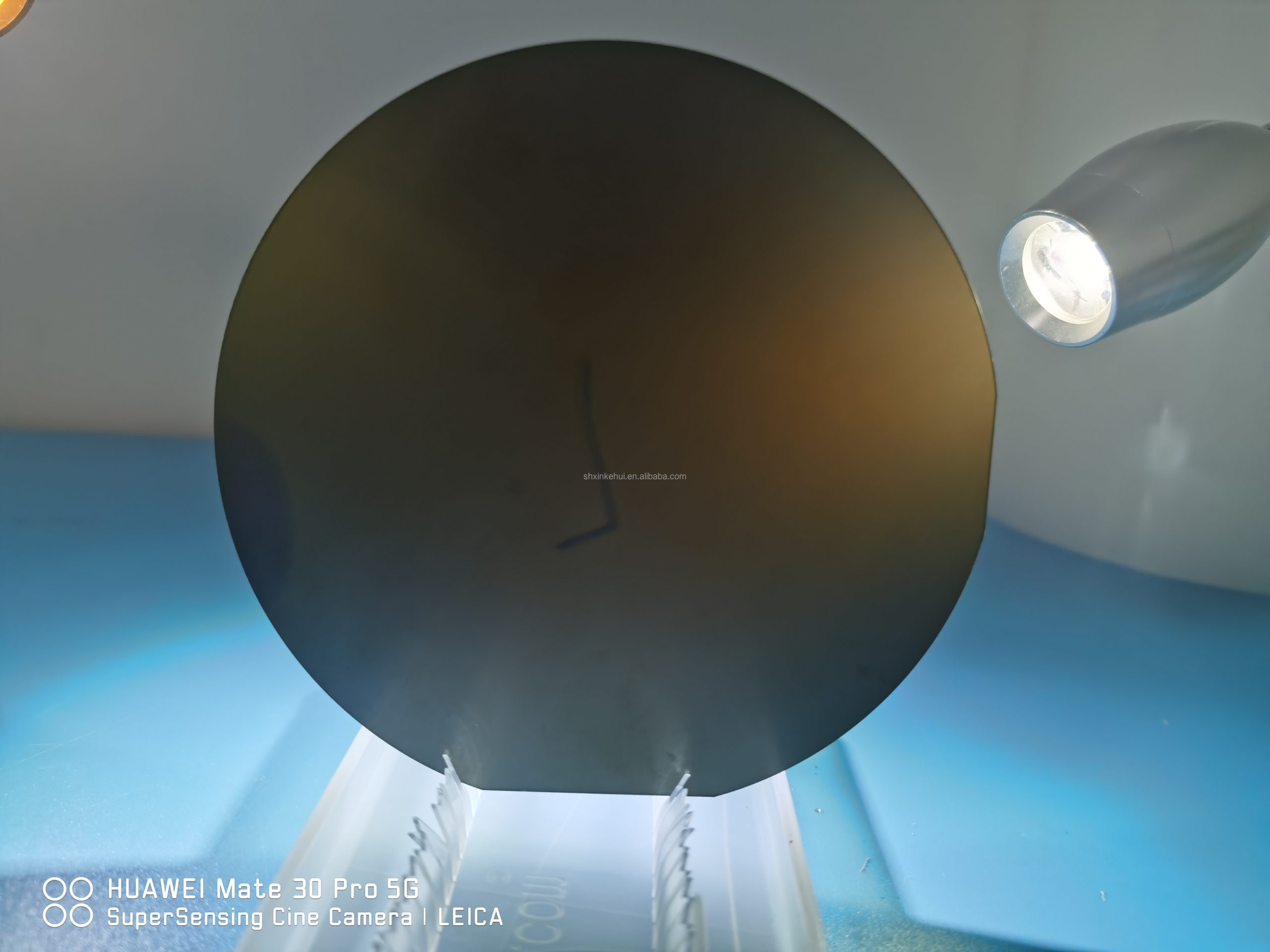
- 6inch 150mm Silicon Carbide SiC Wafers 4H-N type for MOS or SBD Production Research and Dummy grade xinkehui 10*10*0.5 mm Semi P Grade 4H-N Semi SiC Chips Silicon Carbide Wafer


